RP2040
The Pico-compatible part of the UDOO KEY is built upon a Raspberry Pi RP2040 microcontroller, dual Arm Cortex-M0+, with a QSPI 8MB Flash, a 133MHz clock and 264KB of on-chip SRAM. The RP2040 microcontroller is a chip from Raspberry Pi Foundation that integrates two Arm Cortex-M0+ CPUs that can be run up to 133MHz, featuring 264kB of on-chip SRAM and up to 16MB of off-chip Flash memory. This microcontroller can be used for machine learning, motor control, audio and so on. The UDOO KEY is 100% compatible with Raspberry Pi Pico both hardware and software-wise. This means that each and any expansion hardware as well as each and any software built for Raspberry Pi Pico will work out of the box on UDOO KEY. For further information on RP2040, please refer to the dedicated page on raspberrypi.com.
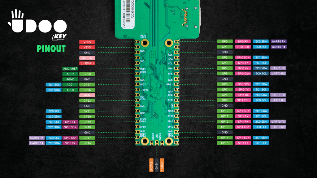
P1 and P2 connectors of the Pico part can be used to connect external peripherals to the RP2040. Two 20-pin headers or castellated holes must be soldered on P1 and P2 in a proper manner to use them . The following tables summarize the possibilities offered by P1 and P2 connectors.
P1
| Pin number | Schematic pin name | SPI | UART interface | I²C | PWM | SIO/PIO |
|---|---|---|---|---|---|---|
| 1 | N.C. | - | - | - | - | - |
| 2 | N.C. | - | - | - | - | - |
| 3 | GND | - | - | - | - | - |
| 4 | RPI_SDA | SPI0_SCK | UART0_CTS | I2C1_SDA | PWM1_A | SIO/PIO0/PIO1 |
| 5 | RPI_SCL | SPI0_TX | UART0_RTS | I2C1_SCL | PWM1_B | SIO/PIO0/PIO1 |
| 6 | GP4 | SPI0_RX | UART1_TX | I2C0_SDA | PWM2_A | SIO/PIO0/PIO1 |
| 7 | GP5 | SPI0_CSn | UART1_RX | I2C0_SCL | PWM2_B | SIO/PIO0/PIO1 |
| 8 | GND | - | - | - | - | - |
| 9 | GP6 | SPI0_SCK | UART1_CTS | I2C1_SDA | PWM3_A | SIO/PIO0/PIO1 |
| 10 | GP7 | SPI0_TX | UART1_RTS | I2C1_SCL | PWM3_B | SIO/PIO0/PIO1 |
| 11 | GP8 | SPI1_RX | UART1_TX | I2C0_SDA | PWM4_A | SIO/PIO0/PIO1 |
| 12 | GP9 | SPI1_CSn | UART1_RX | I2C0_SCL | PWM4_B | SIO/PIO0/PIO1 |
| 13 | GND | - | - | - | - | - |
| 14 | GP10 | SPI1_SCK | UART1_CTS | I2C1_SDA | PWM5_A | SIO/PIO0/PIO1 |
| 15 | GP11 | SPI1_TX | UART1_RTS | I2C1_SCL | PWM5_B | SIO/PIO0/PIO1 |
| 16 | GP12 | SPI1_RX | UART0_TX | I2C0_SDA | PWM6_A | SIO/PIO0/PIO1 |
| 17 | GP13 | SPI1_CSn | UART0_RX | I2C0_SCL | PWM6_B | SIO/PIO0/PIO1 |
| 18 | GND | - | - | - | - | - |
| 19 | GP14 | SPI1_SCK | UART0_CTS | I2C1_SDA | PWM7_A | SIO/PIO0/PIO1 |
| 20 | GP15 | SPI1_TX | UART0_RTS | I2C1_SCL | PWM7_B | SIO/PIO0/PIO1 |
Pin number 1 and 2 are not connected since are used for MCUs communication.
P2
| Pin number | Schematic pin name | SPI | UART interface | I²C | PWM | SIO/PIO |
|---|---|---|---|---|---|---|
| 1 | GP16 | SPI0_RX | UART0_TX | I2C0_SDA | PWM0_A | SIO/PIO0/PIO1 |
| 2 | GP17 | SPI0_CSn | UART0_RX | I2C0_SCL | PWM0_B | SIO/PIO0/PIO1 |
| 3 | GND | - | - | - | - | - |
| 4 | GP18 | SPI0_SCK | UART0_CTS | I2C1_SDA | PWM1_A | SIO/PIO0/PIO1 |
| 5 | GP19 | SPI0_TX | UART0_RTS | I2C1_SCL | PWM1_B | SIO/PIO0/PIO1 |
| 6 | GP20 | SPI0_RX | UART1_TX | I2C0_SDA | PWM2_A | SIO/PIO0/PIO1 |
| 7 | GP21 | SPI0_CSn | UART1_RX | I2C0_SCL | PWM2_B | SIO/PIO0/PIO1 |
| 8 | GND | - | - | - | - | - |
| 9 | GP22 | SPI0_SCK | UART1_CTS | I2C1_SDA | PWM3_A | SIO/PIO0/PIO1 |
| 10 | RPI_RESET | - | - | - | - | - |
| 11 | GP26 | SPI1_SCK | UART1_CTS | I2C1_SDA | PWM5_A | SIO/PIO0/PIO1 |
| 12 | GP27 | SPI1_TX | UART1_RTS | I2C1_SCL | PWM5_B | SIO/PIO0/PIO1 |
| 13 | GND | - | - | - | - | - |
| 14 | GP28 | SPI1_RX | UART0_TX | I2C0_SDA | PWM6_A | SIO/PIO0/PIO1 |
| 15 | ADC_VREF | - | - | - | - | - |
| 16 | 3V3 | - | - | - | - | - |
| 17 | N.C. | - | - | - | - | - |
| 18 | GND | - | - | - | - | - |
| 19 | VSYS | - | - | - | - | - |
| 20 | VBUS | - | - | - | - | - |
Pin number:
- 10 is reserved for RP2040 reset by ESP32
- 16 provide 3.3V DC (315mA) in output
- 17 is not connected
- 19 provide 5V DC (500mA) filtered from USB Type-C connector (CN1)
- 20 provide 5V DC (500mA) raw from USB Type-C connector (CN1)
P5
The Serial Wire Debug interface is available on the 1x3 poles connector P5. This header allows you to program and debug the RP2040 microcontroller externally.
The following table shows the pin configuration.
| Pin number | Function |
|---|---|
| 1 | SWCLK |
| 2 | GND |
| 3 | SWDIO |